 Environmental Technology Co., Ltd.")


Over the past 50 years, the technology node for integrated circuits has decreased significantly from 10 micrometers (μm) in 1971 to the current 7 nanometers (nm), and is even advancing to the smaller 3nm node. The miniaturisation of critical dimension of semiconductor wafer has led to increasingly stringent requirements for the cleanliness of cleanroom production environments. Airborne Molecular Contaminants (AMCs) have gradually replaced particulate pollutants as one of the key factors affecting the productivity of industrial processes.
AMC may lead to many potential process problems, such as Molecular Acids (MA), which are corrosive and will corrode the metal film on the wafer. It will cause pits, open lines, short circuits, leakage, and other defects. Molecular Bases (MB), the existence of ammonia gas will produce photolithography pattern defects and will lead to T-topping on the top of the photoresist line. Molecular Condensables (MC) can easily adhere to the surface of the silicon wafer, forming a thin film and Surface Molecular Contamination (SMC), creating a photoresist layer, sputtering layer, PVD layer or CVD layer that will sandwich the structure. In addition, the volatile VOCs containing silicon, phosphorus, boron, etc., such as siloxane, organophosphate, etc., will be absorbed and firmly stuck to the surface of the silicon wafer, lithography machine lens or lithography plate and removing them can be very hard or impossible. They are referred to as refractory compounds by lithography engineers. Molecular Dopants (MD) such as organophosphate will decompose into inorganic phosphide and become dopants after heating if it absorbs to the surface of the silicon wafer. It will cause undesired n type doping which will lead to voltage drift and other problems.
The semiconductor production process includes sophisticated microelectronic systems and ICs, and the requirements for the cleanliness of the production environment are stringent. Therefore, the entire manufacturing process is carried out under strictly controlled environmental conditions, known as a cleanroom.
The semiconductor clean workplace usually adopts a vertical unidirectional flow method. It exhausts the indoor polluted air to the outside through the push-out function to maintain the cleanliness of the cleanroom. The process is vital for purifying the indoor air.
Cleanroom air purification is mainly divided into three stages:
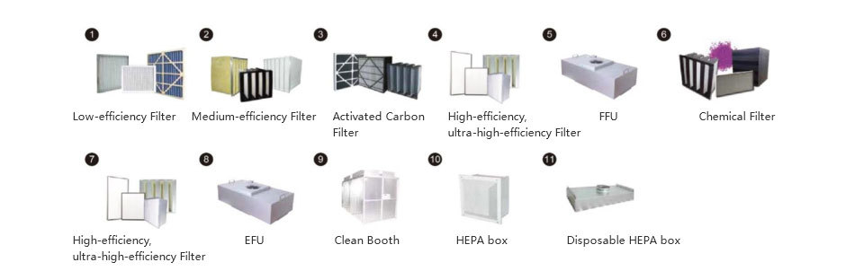
In the first stage, the outside air is filtered through multiple stages, including a pre-filter, a low-medium efficiency filter, a high-efficiency filter, and a chemical filter housed in an air-condition casing. These filters help remove various floating objects and particles with diameters larger than 0.3µm and chemical pollutants from the atmosphere step by step;
In the second stage, through the fan filter unit and the built-in (or matched) high-efficiency, ultra-high-efficiency filter and chemical filter (when the process requires), a stable laminar flow of clean air is pushed into the cleanroom. The atmosphere is purified and meets extremely high cleanliness standards;
In the third stage, the returning air of the cleanroom is sent to the fan filter unit through the raised floor and the air supply duct (or returning air channel). After going through the high-efficiency, ultra-high-efficiency, and chemical filters, it is then sent back to the cleanroom.
The schematic diagram of the main structure of the MayAir semiconductor clean workshop and the application process of the main products are as follows:
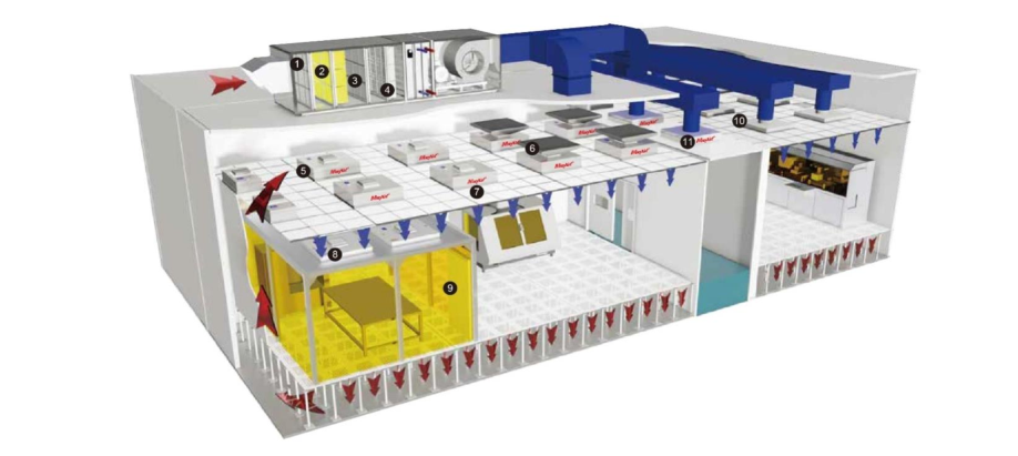
The outside air enters the internal circulation system of the cleanroom after being filtered step-by-step through multi-stage air filters (No. 1 to 4). Afterwards, the clean air is sent to the interior of the cleanroom in a stable laminar flow through the fan filter unit with a high-efficiency/ultra-high-efficiency filter and optional chemical filter (No. 5, 6, 7). The uninterrupted operation of the fan filter unit maintains consistent cleanliness in the work area. In specific equipment or work areas with higher cleanliness requirements, the air is further purified inside the cleanroom through the purification booth with EFU (No. 8, 9) to achieve a higher level of cleanliness in a confined area.
Since receiving the first OBM FFU order from Chengdu SMIC in 2005, MayAir has contributed to the development of China’s semiconductor industry and carved a niche in the high-end cleanroom field.


