banner

N E W S

新闻中心

Technology | Why have silicon wafer factories become more and more strict with AMC (Airborne Molecular Contamination) control in recent years?

  • Time of issue:2022-06-10

(Summary description)Silicon Wafer is often used as a substrate material for semiconductor electronic devices. It is a key component and high-cost upstream raw material for manufacturing chips in the semiconductor industry. Indeed, it is a vital component for all electronic products, such as computers, communications products, automobiles, consumer electronics, etc.

Technology | Why have silicon wafer factories become more and more strict with AMC (Airborne Molecular Contamination) control in recent years?

(Summary description)Silicon Wafer is often used as a substrate material for semiconductor electronic devices. It is a key component and high-cost upstream raw material for manufacturing chips in the semiconductor industry. Indeed, it is a vital component for all electronic products, such as computers, communications products, automobiles, consumer electronics, etc.

  • Categories:Application
  • Author:
  • Origin:
  • Time of issue:2022-06-10 18:12
  • Views:
Information

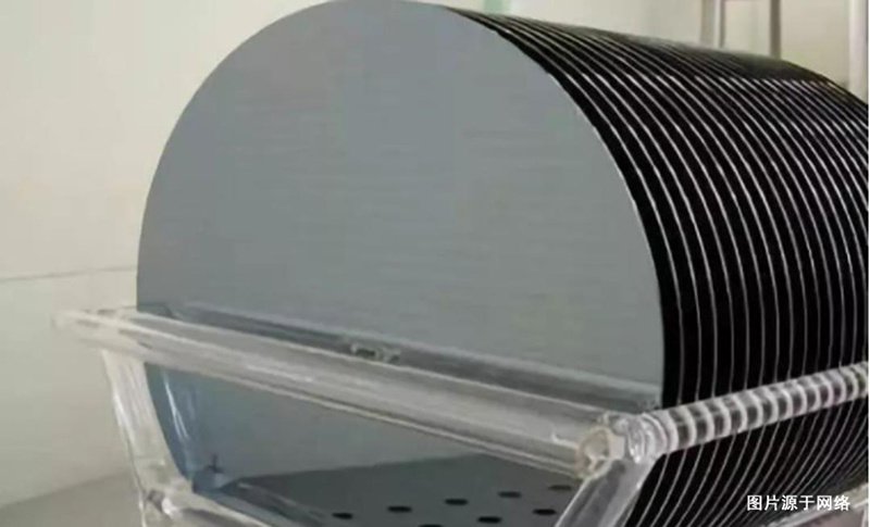
What is silicon wafer?

Silicon Wafer is often used as a substrate material for semiconductor electronic devices. It is a key component and high-cost upstream raw material for manufacturing chips in the semiconductor industry. Indeed, it is a vital component for all electronic products, such as computers, communications products, automobiles, consumer electronics, etc.


1


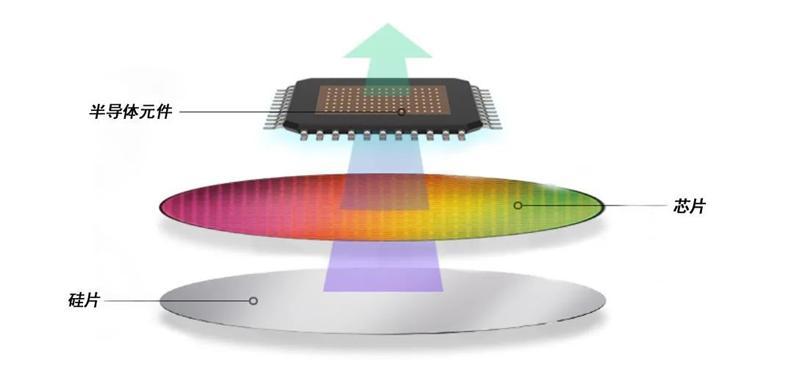
The manufacture of silicon wafers are drawn and refined from ordinary silica sand. After the sand has passed through a series of steps in dissolving, purifying and distilling, single crystalline silicon rods are created. The single crystalline silicon rods are sliced, etched, polished, cleaned and packaged to produce silicon wafers that meet the performance requirements of their semiconductor fabs.


=


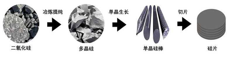
Silicon wafer manufacturing process

The diameter of the silicon wafer has been developed from the 1 inch in 1960 to the matured 12-inch technology of today. The larger the diameter, the more chips can be produced on the same wafer, so that the final cost of a single chip is lower. However, the larger the diameter, the higher the technical requirements for the production and processing of materials, such as the issues of uniformity and purity. This is especially so for semiconductor-grade silicon wafers used in chip manufacturing, the silicon purity is required to reach 99.999999999%.


1


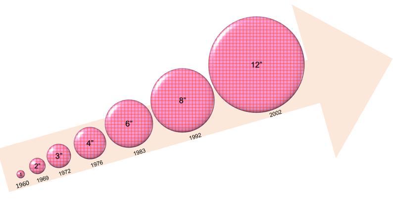
Silicon wafer diameter size development

Wafer Manufacturing and Development

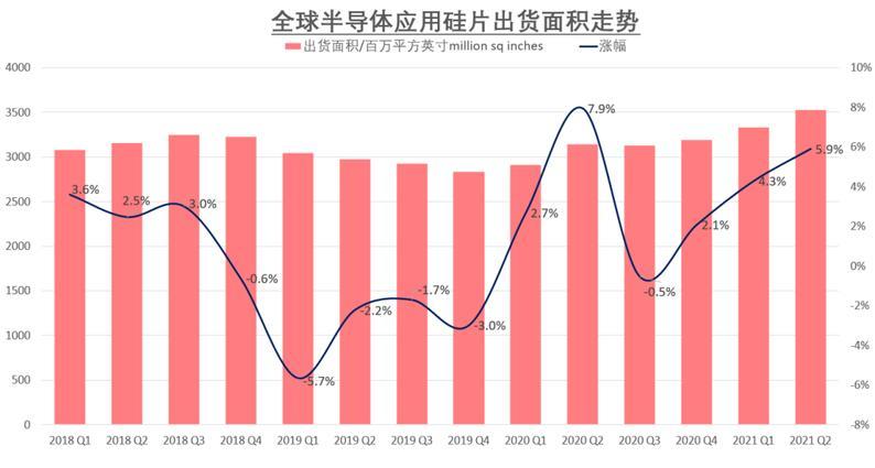
Since the second half of 2020, the capacity of the global foundry market has continued to be in short supply, which has also boosted the demand for semiconductor silicon wafers. According to the latest quarter of wafer industry analytical report from the Silicon Manufacturers Group (SMG), a subsidiary of the International Semiconductor Equipment Association (SEMI), the global silicon wafer shipment in area has increased by 6% in the second quarter of this year compared with the previous quarter. It had reached an area of 3,534 million square inches (MSI), and had surpassed historical record of 3,337MSI in the previous quarter. Again, reaching a new high record, it has increased by 12% in like comparison to 3,152MSI, from the same quarter of previous year to 2020Q2. In addition to the continuous tight supply of 12-inch large silicon wafers for logic chips, the rapid growth of applications such as automotive electronics has also led to a shortage of 8-inch silicon wafers. However, the growth in the supply of semiconductor silicon wafers is relatively slow. Thus, this exacerbates the supply shortage of global semiconductor.


=


Domestic wafer manufacturers emerge, shatters the silicon wafers monopoly stronghold

Due to challenges, such as high degree of technical difficulty, long R&D cycle, huge investment capital outlay and long customer certification cycle, existing in the semiconductor wafer industry, the global wafer market is oligopolized by the top five wafer manufacturers, with a market share of nearly 90%. In the silicon wafer manufacturing process, the focus on single crystal growth technology is to ensure that the drawn silicon ingot maintains an extremely high purity level, while effectively controlling the density of crystal defects. In the production process, in addition to good control of resistivity, flatness, particles, COP, metal contamination, etc., Airborne Molecular Contamination (AMC) is also a part of the control measure. This is to ensure that product defects due to defective silicon wafers will not occur, in the process of manufacturing integrated circuit wafers, when silicon wafers are delivered to downstream customers for use.


=


Safeguarding the environment for extreme manufacturing process of semiconductors

In the past few years, with the large-scale mass production of 12-inch large silicon wafers in China, the production capacity of domestic large silicon wafers has also continued to increase, and silicon wafer manufacturers have also realized that the control of AMC is a key driver in improving product yield. Relying on more than 20 years of experience in semiconductor wafer factories at home and abroad, MayAir AMC Chemical Filtration Division provides AMC solutions and helps customers to improve their product yields, as well as contributes to the local wafer industry, and breaks the monopoly stronghold of imported wafers into China's large semiconductor wafer material market. MayAir’s track record experience includes serving overseas wafer factories such as MEMC, and also several leading domestic wafer factories, such as National Silicon Industry Group Co,. Ltd, Zhonghuan Semiconductor Co., Ltd., Wafer Works Corporation, and Ferroctec.

Innovation, breakthrough, bottleneck challenges, yes we can! MayAir has always adhered to the responsibility of air purification. In the future, we will continue to develop towards the direction of specialisation and intelligence, to meet the various high-end customisation needs put forward by customers, and to help the semiconductor industry to continue to expand.

Recommended information

Technology | Why have silicon wafer factories become more and more strict with AMC (Airborne Molecular Contamination) control in recent years?
Silicon Wafer is often used as a substrate material for semiconductor electronic devices. It is a key component and high-cost upstream raw material for manufacturing chips in the semiconductor industry. Indeed, it is a vital component for all electronic products, such as computers, communications products, automobiles, consumer electronics, etc.
See more information 白箭头 黑箭头
Good News | MayAir has won the third prize for Jiangsu Science and Technology Award
Recently, the Science and Technology Department of Jiangsu Province announced the results of the 2021 Jiangsu Science and Technology Award. MayAir Technology (China) Co., Ltd. (hereinafter referred to as "MayAir"), being the unit to complete with a second achievement for "Key Technology and Application of High Efficiency and Low Resistance Bacteria of Glass Microfiber Air Filter Material", had won the third prize.
See more information 白箭头 黑箭头
BeiGene and MayAir Protecting you - Hundreds of Innovative Drugs, Benefitting The World and Humanity
In recent years, with the outbreak of the COVID-19 epidemic, the demand for antibody drugs in the pharmaceutical field has increased. Benefiting from the reform of the drug review and approval system, the barriers to production capacity, output, technology, etc. of various pharmaceutical companies have continued to be considerably reduced. Our country's antibody-drug industry has also achieved rapid growth. Among them, monoclonal antibody drugs play a pivotal role in treating tumours, autoimmunity, metabolism, viral infection, and other diseases because of their high ability to target effectively and precisely. MayAir provided a full range of environmental process protection to construct the local A-level environmental monoclonal antibody drug production project for BeiGene (Guangzhou).
See more information 白箭头 黑箭头
Industrial Application Analysis of Chemical Filters in the Semiconductor Industry - RC Insoluble Compounds Control
The project is for a semiconductor design and manufacturing enterprise in Zhejiang, which is headquartered in Hangzhou. The company focuses on the design and manufacture of memory chips and related chips, and provides semiconductor chips and application solutions for the Internet of Things, smart transmission terminals, industrial control and automotive electronics.
See more information 白箭头 黑箭头
MayAir is helping to build Dana's smart cabins, and showcase their skills in pandemic prevention and control
Recently, the mutated strain of Omicron has been spreading widely around the world. Thus, the global new covid-19 pneumonia pandemic situation has once again entered into an intense stage. In response to the urgent need for clinical gene amplification nucleic acid testing of the new coronavirus, and to satisfy the prerequisite for biosafety requirements in clinical testing, the need for pandemic prevention and control, with efficiency and rapid deployment features, have been combined to satisfy the supply needs of biosafety laboratories for the prevention and control of the new covid-19 pandemic and for future public health events. China rapidly established shelter-type and mobile nucleic acid testing laboratories have played an important role in improving nucleic acid testing capabilities, expanding testing coverage, and assisting the public in pandemic prevention and control.
See more information 白箭头 黑箭头
Exhibition: Autumn at Chengdu, The Pharmaceutical Grand Event
The 61st China National Pharmaceutical Machinery Exposition (Autumn 2021) was officially launched at the Chengdu Western International Expo City, China, on Nov. 2, 2021. This event fulfilled the industry’s expectations and gained national attention, where it focused on pharmaceutical equipment and integrated the industry’s high-quality resources.
See more information 白箭头 黑箭头
Exhibition: The National Hospital Construction, Equipment and Management Exhibition Concluded Successfully
The grand opening of the 22nd National Hospital Construction, Equipment and Management Exhibition (the Hospital Construction Exhibition) was held successfully at the Shenzhen International Convention and Exhibition Centre. MayAir showcased a variety of medical-grade purification products that successfully combined purification technology with hospital construction.
See more information 白箭头 黑箭头
New Product Launch | Stay tuned September
See more information 白箭头 黑箭头

Search

搜索
Search

Promote the development of purification industry and improve global air quality

公众号二维码

WeChat